- PCB Blog
- Future Trends of Flexible Circuit Boards
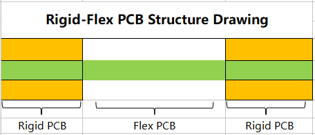
- Rigid-Flex PCB Stack-up for Impedance Controlled Designs
- Control Impedance Between Rigid PCB and Flex PCB
- Flex PCB Reliability and Bendability
- Normal Flex PCB Specifications
- Flex PCB Polyimide Coverlay and Solder Mask
- Flex PCB Boards and Connectors
- About RA Copper and ED Copper
- Introduction of Flexible PCB
- 5 Tips For Designing Flexible PCB
- Advantages of FPC (Flexible PCB)
- Evolution of the Flex Printed Circuit Board
- Benefits of Using Flex Circuit Boards
- Why Rigid-Flex PCBs are Economical?
- Flexible PCB vs Rigid PCB
- Development of Flexible printed circuit board (FPC) market
- Traditional Manufacture Engineering of FPC Substrate
- Development Trend of FPC Board
- Flex PCB and the Manufacturing
- About Flex PCB design
- About Flex PCB and Assembly
- How to Ensure Flex PCB Design Success
- How to Select the Appropriate FPC Materials?
- The Differences In Rigid PCB, Flex PCB and Rigid-Flex PCB
- Flex-Rigid PCB Design Guidelines
- Beneficials for Polyimide Flex PCB Boards
- About Stiffener on Flex PCB FPC circuit Boards
- About ENIG and ENEPIG
- PCB Surface Finish Comparison
- Copper Thickness for FPC Boards
- Interconnect Solutions for Flexible Printed Circuits and Etched Foil Heaters
- Advantages and Disadvantages of Rigid-Flex PCB
- About FPC Plating Process
- About EMI shield design for Flex Printed Circuit Board
- PCB Assembly Blog
In recent years, 3D packaging technology has become a research hotspot, which has attracted the attention of many large semiconductor companies, and now there are practical products.
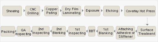
Traditional Manufacturing Engineering of Flexible Substrate:
Traditional manufacturing processes of flexible substrates include “Roll Reduction Method” and “Sheet Metal Processing Method”. Different manufacturing methods have different characteristics, but the most common manufacturing method is “Sheet Metal Processing Method”. Figure 1 shows the manufacturing flow chart of double-sided flexible substrate processing method.
The blanking process in the manufacturing process of flexible substrates is different from that of rigid substrates. In addition to the blanking of CCL and cover plates, the blanking of cladding and reinforcing panels is also added. Flexible CCL and cladding are rolled, so we need to use automatic blanking machine when using. In the manufacturing process of flexible substrates, the fouling removal technology of drilling holes is also different from that of rigid substrates. According to the provisions of IPC-A-600F, the depth of concave corrosion in the fouling removal process of flexible substrates shall not exceed 50um. However, polyimide is not resistant to strong alkali, and the strong alkaline potassium permanganate solution commonly used in rigid substrates is no longer suitable for the processing of flexible substrates.
In order to ensure the decontamination effect and concave corrosion depth meet the requirements, plasma is generally used in the industry for decontamination and concave corrosion. In the PTH process, it usually uses the alkaline solution.Due to the long-term reaction will cause FPC material swelling, which will lead to holes and poor mechanical properties of the coating, such as ductility and adhesion. At this time, the substrate material is very easy to break under thermal shock, so generally after the thickness of the copper layer during the PTH process reaches 0.3 to 0.5um, it is transferred to the electroless plating of the whole board until its thickness reaches to 3 to 4um, in order to ensure the integrity of the copper layer of hole wall in the subsequent processing process.
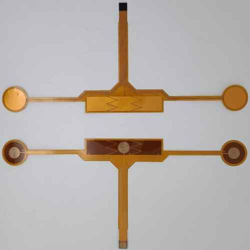
In terms of line production, flexible substrate etching is slightly different from rigid substrate. In general, a large number of parallel wires are designed at the bending part. In order to ensure the consistency of etching, the spraying direction, pressure and transmission direction of etching solution should be appropriately adjusted during etching. Etched circuit boards are treated to increase adhesion prior to aligning the overlay. The cladding layer after drilling and the etched flexible circuit board have different degrees of moisture absorption, so these materials should be dried in the drying oven for 24 hours before lamination, stack height should not exceed 25 um. In the case of the PCB etched by the covering layer, a special alignment fixture or a visual magnifying glass can be used for alignment. After alignment, butanone or hot flame iron can be used for positioning.
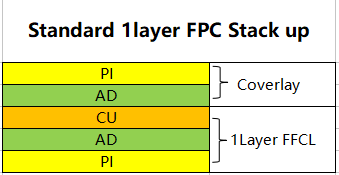
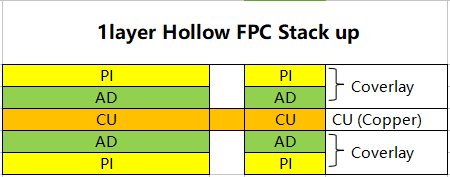
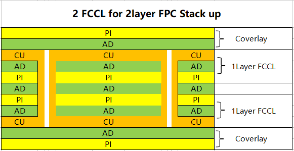
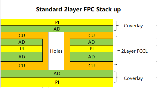
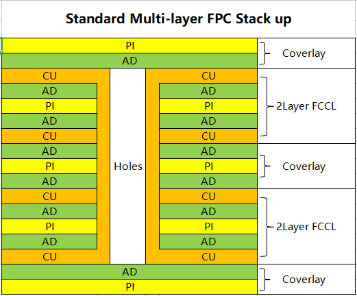
According to different FPC materials to determine the lamination time, heating rate and pressure and other lamination process parameters, flexible multilayer substrate lamination ratio than rigid substrate complex, the substrate, adhesive and gasket material matching window is relatively narrow, only the correct choice of materials and appropriate processing parameters can achieve the ideal lamination effect. Pictue below shows the FCCL and the FPC stack-up.
| FCCL Material Thickness | ||||
| Coverlay/Solder Mask | 2Layer FCCL | |||
| PI (12.5/25/50/100um, etc.) | Copper (6/9/12/18/35/70/100um, etc.) | |||
| AD (15/25/35/50um, etc.) | AD (0/12.5/20/25um, etc.) | |||
| PI (12.5/25/50/100um, etc.) | ||||
| 1Layer FCCL | AD (0/12.5/20/25um, etc.) | |||
| Copper (6/9/12/18/35/70/100um, etc.) | Copper (6/9/12/18/35/70/100um, etc.) | |||
| AD (0/12.5/20/25um, etc.) | ||||
| PI (12.5/25/50/100um, etc.) | ||||
| Flex PCB Stack-up Structure | |
 |  |
 |  |
 |  |